
Khaberni - Nvidia has succeeded in leading the global companies in terms of market value, driven by the massive demand for its advanced chips that power the artificial intelligence revolution.
However, this remarkable success would not have been possible without a less well-known European company, but of great importance in the semiconductor industry, which is the Dutch company "ASML".
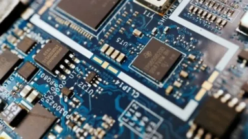
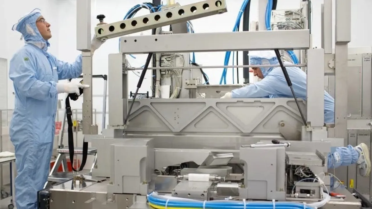
"ASML" is one of the most valuable technology companies in Europe, specializing in manufacturing photolithography machines used in etching the finest patterns on silicon wafers, a crucial step in producing advanced electronic chips.
The Dutch company is unique in the world as the only manufacturer of photolithography machines using extreme ultraviolet (EUV) technology, essential for producing the most advanced chips.
"ASML" controls about 90% of the global photolithography market, according to a report published by "CNBC" and reviewed by "Al Arabiya Business".
Market analysts see "ASML"'s dominance as likely to expand.
Didier Schema, an analyst at "Bank of America", predicted that the company would become the actual monopolist in the next generation of EUV technologies, confirming that this technology will support the most prominent technical transformations during this decade.
These forecasts followed the announcement of "ASML"'s business results, which showed that new orders in the fourth quarter of 2025 exceeded analysts' expectations by double.
Catching up with "ASML" is nearly impossible
Meanwhile, Javier Correnero, an equity analyst at "Morningstar", said that photolithography represents the fundamental building block for any electronic chip, indicating that "ASML" machines were involved in manufacturing about 99% of the semiconductors around the world.
He added that EUV technologies specifically are the cornerstone in building the current and future artificial intelligence infrastructure.
"ASML" produces two types of these machines:
Low numerical aperture EUV, used in manufacturing the current generation of artificial intelligence chips, like Nvidia's Blackwell chips.
High numerical aperture (High NA) EUV, which is more advanced and is currently used in research and development laboratories to produce the next generation of chips.
These systems rely on firing powerful laser beams at droplets of molten tin inside a vacuum, creating a plasma that emits EUV light, which is then directed through ultra-precise mirrors to etch chip designs onto silicon wafers.
These machines are sold to chip manufacturing companies such as Taiwanese "TSMC", which in turn works with chip design companies, led by "Nvidia".
Correnero explained that competitors such as the Japanese "Nikon" and "Canon" are still far from this level of development, stating that the investment and technological gap built by "ASML" over three decades makes catching up with them nearly impossible.
Growth Prospects
Company data showed that EUV systems constituted the largest share of new order value, contributing about 7.4 billion euros out of a total of 13.2 billion euros in the fourth quarter of 2025.
Throughout the year, "ASML" sold about 48 EUV systems and generated revenues of 11.6 billion euros.
Although the company does not officially announce the prices of its devices, analysts estimated the price of an advanced High NA EUV system to be between 320 and 400 million euros, while the price of a Low NA EUV system is about 220 million euros.
Companies such as "TSMC", "Intel", and "Samsung" are currently conducting trials on High NA EUV systems inside laboratories, with expectations to enter large commercial production between 2027 and 2028, with "Intel" being one of the first adopters.